Field-effect transistors (FETs) offer some of the most energy-efficient switching in commercial computing chips.
Yet even when operating with minimum possible voltages, FETs still consume too much power to support the accelerating computational demands of advanced technologies and respond to the energy crisis’ appeals for lower-power hardware.
Researchers from the University of Pennsylvania’s School of Engineering and Applied Science have redesigned FETs with these energy imperatives in mind.
Creating devices that harness physics in ways unlike those used in commercial transistors, Penn engineers have nearly halved the amount of voltage needed for switching.
The new logic device design is the subject of a recently published study in Nature Electronics that was co-led by Deep Jariwala, Assistant Professor in the Department of Electrical and Systems Engineering (ESE), and Jinshui Miao, former postdoctoral researcher in ESE and current professor at the Shanghai Institute of Technical Physics, along with Chloe Leblanc and Xiwen Liu, Ph.D. students in ESE. The team worked in collaboration with researchers from the National Institute of Standards and Technology, the Chinese Academy of Sciences, Theiss Research and the Air Force Research Laboratory.
“Computing devices today contain so many transistors—tens of billions—that even a small reduction in energy usage would make a big difference,” says Jariwala. “Our results with this design represent a big reduction, which means the impact on overall energy efficiency will be huge. It undercuts current theoretical minimums by an astonishing amount.”
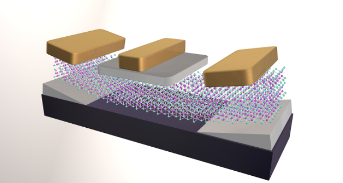
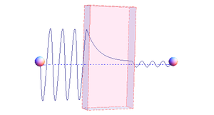
The device, called a TFET (pronounced tee-fet), relies on a physical property known as tunneling. Particles tunnel when they move through energy barriers rather than over them.
“Imagine an electron moving through a FET like a ball that needs to roll up a hill in order to get to the other side,” says Leblanc. “In a TFET, the ball doesn’t need to roll up the hill—it gets a little push and manages to tunnel through it instead. What’s exciting about this study is that we can confirm through multiple device demonstrations and simulations that this physics, the electron tunneling, is definitely the reason our transistor is so effective at low power.”
Tunneling requires much lower voltages than the thermal injection used in state-of-the-art FETs.
Scientists have been experimenting with tunneling FET technology for decades but have been hindered by insurmountable trade-offs in power and performance. Until now, TFETs were able to either operate below the theoretical voltage minimum (60mV/decade, a metric known as the Boltzmann limit) or with sufficient current density at the drain terminal to drive applications at the circuit and system levels. The Penn Engineering research team’s design does both.

“By finally overcoming that trade-off, we have cleared a path for the future integration of TFETs into high-performance, low-power microelectronics,” says Jariwala. “Central to our solution is an experimental new semiconductor called indium selenide (InSe), which is clean enough in terms of crystal quality and achieves high-drive current density. Now that we have a structure that allows for both high current density and low voltage, we can start to build a strong case for substituting a standard FET with a TFET.”
The experiments point to a promising future for TFETs beyond their energy efficiency.
“With future development, these devices have the potential to surpass further FET limitations in size and switching speed,” says Miao. “Our TFET design can likely be miniaturized to degrees that a standard FET cannot and accomplish even faster switching. It’s a very promising solution not only for energy usage, but also other versatile device applications requiring complex computational tasks.”