The microscopic components that make up computer chips must be made at staggering scales. With billions of transistors in a single processor, each made of multiple materials carefully arranged in patterns as thin as a strand of DNA, their manufacturing tools must also operate at a molecular level.
Typically, these tools involve using stencils to selectively pattern or remove materials with high fidelity, layer after layer, to form nanoscale electronic devices. But as chips must fit more and more components to keep up with the digital world’s growing computational demands, these nanopatterning stencils must also become smaller and more precise.
Now, a team of Penn Engineers has demonstrated how a new class of polymers could do just that. In a new study, the researchers demonstrated how “multiblock” copolymers can produce exceptionally ordered patterns in thin films, achieving spacings smaller than three nanometers.
The team, led by Karen Winey, Harold Pender Professor in the Departments of Materials Science and Engineering and Chemical and Biomolecular Engineering, and Jinseok Park, a graduate student in her lab, published these findings in the journal ACS Central Science. They collaborated with Anne Staiger and Professor Stefan Mecking of the University of Konstanz, Germany.
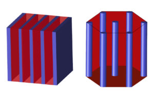
The stencils used in fabricating chips have nanoscale patterns that can be produced by a variety of methods. For example, fine lines and small dots can be produced by a technique known as directed self assembly (DSA), where the polymer chemistry is designed such that it automatically produces the desired geometry.
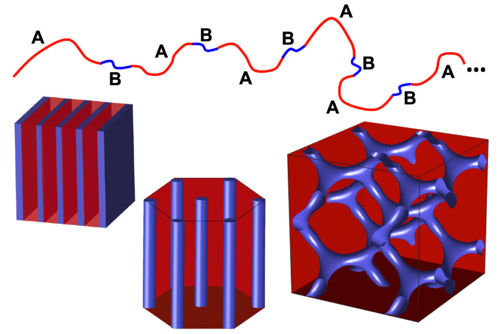
Current DSA methods use “diblock” copolymers, named for having two long blocks of different polymers bonded end to end, which then assemble to produce the necessary patterns.
“When photolithography could not go any smaller, DSA with diblock copolymers became important,” says Winey. “But getting the lines or dots you need for nanopatterning requires both blocks to be specific lengths, and that’s still something that’s hard to control precisely.”
Without the correct ratio of lengths, the blocks in a diblock copolymer form lines or dots with some variability in their dimensions, decreasing their usefulness as stencils.
Together, the Penn and Konstanz researchers devised a way to more precisely control this ratio. Instead of sticking two big blocks of different polymers end to end, they use a technique known as “step growth polymerization” to perfectly alternate between two smaller blocks.
“Compared to diblock,” Winey says, “these multiblock copolymers offer a wider range of chemistries and greater molecular control. That’s because every A-block and every B-block are exactly the same length, which will produce greater uniformity in the pattern.”
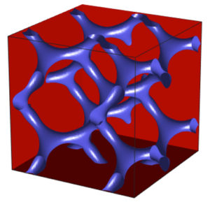
One critical difference this uniformity can make is the ability for the polymer to more easily assemble itself into a “co-continuous double-gyroid structure” within a thin film. This arrangement is particularly useful for controlling transport properties, as it separates the polar and nonpolar regions of the polymers.
“The continuous charged domain can promote conductivity of charged or polar species, like water or ions, and the continuous non-polar domain provides mechanical strength,” says Winey.
The researchers are now investigating how to best convert these thin film structures into functional nanopatterning stencils, as well as developing a library of different multiblock copolymer chemistries that can form double gyroid structures.
The research was supported by the National Science Foundation through grants DMR-1904767 and the Baden-Württemberg Foundation project PRICON. The researchers were able to analyze these structures using the Dual Source and Environmental X-ray Scattering (DEXS) facility housed in Penn’s Laboratory for Research on the Structure of Matter, DMR-17-20530.