As smartphones and laptops get smaller and sleeker in design, so too do the parts that make them. Manufacturing chips and displays in an average smartphone can be a tricky process that increasingly requires integration and assembly of small components. But how can manufacturers pick up and place down very small components to assemble them?
Traditionally, vacuum grippers are used for pick-and-place assembly processes, but they are reaching their limit in terms of how minuscule of an object they can handle.
New solutions are needed to construct the latest technologies, and Penn Engineers have contributed to a collaborative study on using electroadhesion — which exploits the same phenomenon as static cling — to manipulate microscale objects.

The Penn Team was led by Kevin Turner, Professor and Chair of Mechanical Engineering and Applied Mechanics (MEAM), with contributions from members of Turner’s lab: Yijie Jiang, then a doctoral student in MEAM, Kiera Thompson-Towell, then an undergraduate student in Materials Science and Engineering, and Chunxu Chen, then a masters student in MEAM.
The study, led by MIT’s Sanha Kim and A. John Hart, was published in Science Advances.
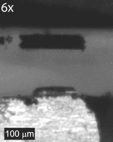
The collaborative research team has developed an electroadhesive stamp that can handle objects with diameters as small as 20 nanometers — about a thousand times thinner than a human hair. The stamp features dielectric-coated carbon nanotubes (CNTs) arranged like bristles on a brush; its stickiness comes from the application of voltage to these CNTs.
This is roughly the same phenomena one experiences when removing clothes from the dryer — as clothes rub together, their friction creates electricity and some material takes on a positive charge while other material takes on a negative charge, causing the pieces of clothing to cling to one another.
Researchers have used CNTs to make “dry” adhesives before, but these CNT-based approaches are usually designed to maximize the contact area to the surface to get strong adhesion. This is the same approach found in nature, such as in gecko feet. Geckos capitalize on the van der Waals force — a weak attractive force between molecules that becomes stronger when two surfaces come into extremely close contact with one another. The notoriously dexterous lizard has feet that are coated with microscopic hairs that bend to maximize contact area and allow them to cling to and climb on both rough and smooth surfaces.
While others have used CNT structures that exploit van der Waals forces to achieve stickiness, the Penn and MIT researchers wanted to turn stickiness on and off, and thus did not want those forces to control the adhesion. To achieve this, the collaborative team took a non-traditional approach: use coated CNTs to create a rough surface that minimizes contact area and apply voltage to the CNTs to create electroadhesion, which can be tuned by the voltage.
The resulting electrostatic stamp can switch the stickiness on and off. When voltage is turned on, the stamp can pick up a minuscule object. When voltage is turned off, the stamp releases it on a given surface. Turner’s group performed experiments to test the adhesion using specialized equipment in their lab and in the Singh Center for Nanotechnology.
“If you’re going to create an adhesive and demonstrate that it’s effective,” Turner says, “You have to measure the adhesion.” Turner’s team used atomic force microscopy to measure the adhesion of their electroadhesive stamp and designed experiments that allowed them to characterize the adhesion of the stamp to micrometer-sized components and quantify it as a function of the applied voltage of the stamp as well as the stamp’s physical design.
“As you change the stamp design,” Turner says, “you obtain different adhesion strengths and we wanted to map how you can tune the adhesion across the design space.”
Turner and his team’s contributions to this collaboration with MIT were focused on understanding the adhesion mechanics and experimentally characterizing the response of the electroadhesive stamps. The outcomes of this research have wide-ranging applications, especially when it comes to manufacturing electronic devices. Small-scale pick-and-place technologies, like this electroadhesive stamp, can be used to integrate high-performance semiconductor materials into wearable and flexible devices, as well as manufacture new types of displays that require the assembly millions of microLEDs on a single backplane. This change could enhance the quality of displays to produce a brighter picture that is more energy efficient than current models. Advances such as this are only possible if they can be manufactured, and this electrostatic stamp could enable electronics manufacturers to create the next generation of sleek, high-performance, and energy-efficient technology.
This research was supported in part by the National Science Foundation, Toyota Research Institute, and the MIT-Skoltech Next Generation Program.
Read more about this research at MIT News.