Dhruv Turakhia: Voices of Penn Engineering Master’s Alumni
This is part of our series of articles, written by Penn Engineering alums in their own words, of their experiences at Penn and how it shaped their lives. Our next article is written by Dhruv Turakhia, who graduated with a master’s in Materials Science and Engineering (MSE) degree in 2015. He currently works in the San Francisco Bay Area as an Inkjet Print Application Engineer at Kateeva.
Growing up in India, a lot of emphasis was placed on quality education and going the extra mile to earn what you want to achieve. Science and technology were areas that I focused my efforts on since the early days of high school, and ultimately I opted for an undergraduate degree in Chemical Engineering from Mumbai University.
I was always fascinated with the world of consumer electronics; I witnessed the revolutionary changes that have come about in mobile phone and TV displays while growing up. From old cathode ray and plasma TV sets to LED and OLED screens, from brick phones to touch screens in smartphones, I was excited and amazed by the vivid colors illuminated in the screens through which we consume a lot of information today.
As I learned more about consumer displays, I realized that the best way for me to work in that field would be to study materials science and technology. Those subjects caught my attention like no other, and I attended various seminars and participated in a range of workshops on them. Slowly and steadily, I also learned about related branches of materials science, such as semiconductors and nanotechnology, and saw how important is it to have these foundations in place to understand the broader aspects of display technology. I believed that graduate study would be the most logical extension of my academic pursuits and a major step towards achieving my objectives.
I was looking for a university in the U.S. and had always heard about the Ivy League. The Materials Science and Engineering program at Penn Engineering was what ultimately caught my eye. The distinguished faculty and excellent facilities gave me a broad exposure to the various branches of the field, namely, semiconductor device technology, nanotechnology, and microelectromechanical systems (MEMS).
The courses that really stood out for me were Semiconductor Device Physics, Nanofabrication/Microfabrication of Devices, and Introduction to MEMS Technology. During my time at Penn, I also undertook a variety of extracurricular activities that aided my growth, such as working as a research assistant in labs where I synthesized and characterized thin film nanocrystals for solar cell applications.
An experience I had at Penn which I will always be grateful for was working as a graduate student fellow (GSF) in the Singh Center for Nanotechnology. The Singh Center is a state-of-the-art research facility that houses a 10,000-square-foot cleanroom with leading-edge equipment that is very important in the semiconductor and display industry. The tools and techniques involved in thin film deposition and characterization form the basis for most current TV and smartphone displays, so the program helped me gain hands-on skills and familiarity with the equipment used in the industry today.
The GSF program also prepares you for life after academics since these are the tools that are very much used in today’s semiconductor and display industries. This entire experience was very rewarding as it made me stand out from other candidates while applying for jobs.
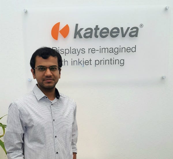
I currently work as an Inkjet Print Application Engineer at Kateeva in the Silicon Valley area of California. Kateeva is a leading developer of manufacturing equipment for OLED screen displays, and I work in a customer-specific role in the Print Technology Group, where I help to troubleshoot and optimize inkjet printing systems and arrange customer demonstrations.
Smartphones, tablets, laptops and large-scale TVs with OLED, or organic light emitting diode, displays have a layer of organic molecules a few hundred nanometers thick that produce light when electricity is applied to it. With inkjet printing, these organic molecules are sprayed onto substrates just like inks are sprayed onto paper by a desktop printer. Inkjet technology greatly reduces the cost of OLED manufacturing and allows OLEDs to be printed over very large areas and even onto flexible displays.
Penn Engineering gave me both theoretical knowledge about semiconductors and nanotechnology and the practical skills related to thin film deposition that forms the basis of the inkjet technology that I work with on a daily basis. It has made me very well rounded and qualified to work on the forefront of this path-breaking technology in an impactful role.
My journey has been very fruitful and exciting, leading to a position in the industry that I always dreamt of working in while growing up. All this goes back to the knowledge and skills I picked up at Penn. The abundance of resources available at Penn, be it the excellent teaching faculty, the research facilities, or the strong alumni network, is something I have utilized to the fullest extent.
In hindsight, I am grateful to have chosen the Materials Science and Engineering program at Penn. I wish to extend heartfelt gratitude and a big thank you to everyone at Penn that has helped my professional development.